 ReddRadar

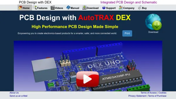
What is AutoTRAX DEX PCB Designer?
AutoTRAX DEX PCB Designer is a comprehensive electronic design automation (EDA) platform that unifies schematic capture, PCB layout, simulation, and manufacturing processes in a single, consistent environment. Its integrated architecture eliminates the need for separate applications and file formats, maintaining electrical integrity throughout the design process and ensuring efficiency from conceptualization to final production.
The software features real-time design rule checking, simulation with interactive instruments, automatic and manual PCB routing, advanced manufacturing file outputs including Gerber and CNC, and sophisticated 3D visualization capabilities. Powerful parametric part creation and unified data management further streamline design workflows for engineers, enabling the rapid creation, iteration, and deployment of next-generation electronic products.
Features
- Unified Platform: Single-application environment for schematic, PCB design, and manufacturing.
- Real-Time Design Rule Checking: Instant notification and correction of design rule violations.
- Parametric Part Creation: Automatic generation of footprints, schematic symbols, and 3D models from parameters.
- Integrated Simulation: Place real instruments such as oscilloscopes and signal generators on schematics with real-time updates.
- Advanced PCB Layout: Autorouting, manual routing, unlimited board size, and unlimited layers.
- Active3D Visualization: Real-time, high-quality 3D graphics, including shadows, transparency, and bump mapping.
- Comprehensive Manufacturing Support: Gerber, CNC, and pick-and-place file generation with built-in viewers.
- Synchronous Design Updates: Changes in schematic automatically reflected in PCB layout and vice versa.
Use Cases
- Designing custom electronic circuit boards for commercial hardware products.
- Educational electronics labs requiring a unified design and simulation environment.
- Electronics prototyping and rapid PCB iteration for startups.
- Industrial control panel or embedded device PCB creation.
- Hardware engineering teams managing complex projects with extensive parts and layers.
- Creating manufacturing-ready CAM files for PCB production.
FAQs
-
What is the main advantage of using AutoTRAX DEX over traditional EDA tools?
AutoTRAX DEX provides a fully unified environment where schematic capture, PCB layout, simulation, and manufacturing processes are integrated, ensuring seamless workflow and real-time synchronization without the need for separate applications or file formats. -
Does AutoTRAX DEX support unlimited board size and number of layers?
Yes, AutoTRAX DEX allows for unlimited board size, layers, parts, pads, and nets, enabling scalable design for both simple and highly complex electronic products. -
Can I generate manufacturing files directly with AutoTRAX DEX?
Yes, the software offers comprehensive manufacturing support, including real-time DRC, full Gerber file output, a Gerber viewer, CNC output with a built-in viewer, and pick-and-place file creation. -
What simulation capabilities does AutoTRAX DEX offer?
AutoTRAX DEX includes integrated XSpice-based simulation, allowing the use of real instruments such as oscilloscopes and signal generators directly within the schematic for interactive, real-time analysis. -
Is documentation available for AutoTRAX DEX?
Yes, users have access to an extensive manual and support resources through the official website.
Related Queries
Helpful for people in the following professions

Featured Tools
Join Our Newsletter
Stay updated with the latest AI tools, news, and offers by subscribing to our weekly newsletter.